- 您现在的位置:买卖IC网 > Sheet目录3878 > PIC18F4610T-I/ML (Microchip Technology)IC MCU FLASH 32KX16 44QFN
2009 Microchip Technology Inc.
DS39636D-page 75
PIC18F2X1X/4X1X
5.5.3
MAPPING THE ACCESS BANK IN
INDEXED LITERAL OFFSET
ADDRESSING MODE
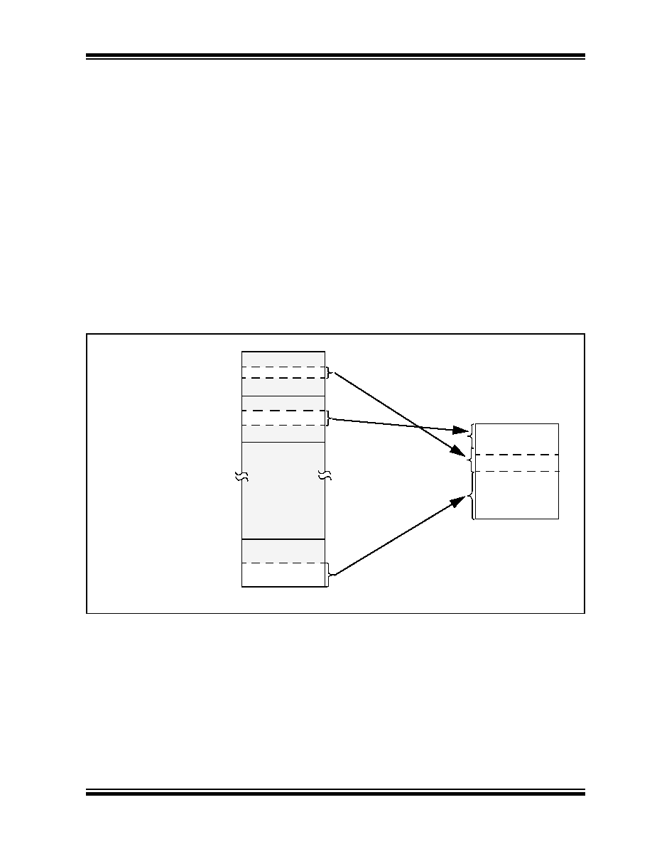
The use of Indexed Literal Offset Addressing mode
effectively changes how the first 96 locations of access
RAM (00h to 5Fh) are mapped. Rather than containing
just the contents of the bottom half of Bank 0, this mode
maps the contents from Bank 0 and a user defined
“window” that can be located anywhere in the data
memory space. The value of FSR2 establishes the
lower boundary of the addresses mapped into the
window, while the upper boundary is defined by FSR2
plus 95 (5Fh). Addresses in the Access RAM above
5Fh are mapped as previously described (see
Section 5.3.2 “Access Bank”). An example of Access
Bank remapping in this addressing mode is shown in
Remapping of the Access Bank applies only to opera-
tions using the Indexed Literal Offset Addressing
mode. Operations that use the BSR (Access RAM bit is
‘1’) will continue to use direct addressing as before.
5.6
PIC18 Instruction Execution and
the Extended Instruction Set
Enabling the extended instruction set adds eight
additional commands to the existing PIC18 instruction
set. These instructions are executed as described in
FIGURE 5-11:
REMAPPING THE ACCESS BANK WITH INDEXED LITERAL OFFSET
ADDRESSING
Data Memory
000h
100h
200h
F80h
F00h
FFFh
Bank 1
Bank 15
Bank 2
through
Bank 14
SFRs
05Fh
ADDWF f, d, a
FSR2H:FSR2L = 120h
Locations in the region
from the FSR2 Pointer
(120h) to the pointer plus
05Fh (17Fh) are mapped
to the bottom of the
Access RAM (000h-05Fh).
Locations in Bank 0 from
060h to 07Fh are mapped,
as usual, to the middle of
the Access Bank.
Special File Registers at
F80h through FFFh are
mapped to 80h through
FFh, as usual.
Bank 0 addresses below
5Fh can still be addressed
by using the BSR.
Access Bank
00h
80h
FFh
7Fh
Bank 0
SFRs
Bank 1 “Window”
Bank 0
Bank 0
Window
Example Situation:
07Fh
120h
17Fh
5Fh
Bank 1
发布紧急采购,3分钟左右您将得到回复。
相关PDF资料
PIC18F4610-E/PT
IC MCU FLASH 32KX16 44TQFP
PIC18F4610-E/ML
IC MCU FLASH 32KX16 44QFN
PIC18LF2331T-I/SO
IC MCU FLASH 4KX16 28SOIC
PIC18F4515T-I/PT
IC MCU FLASH 24KX16 44TQFP
PIC18F4431T-I/ML
IC MCU FLASH 8KX16 44QFN
PIC18F4431-E/ML
IC MCU FLASH 8KX16 44QFN
PIC18F4410T-I/ML
IC MCU FLASH 8KX16 44QFN
PIC18F4410-E/PT
IC MCU FLASH 8KX16 44TQFP
相关代理商/技术参数
PIC18F4610T-I/PT
功能描述:8位微控制器 -MCU 64KB 3968 RAM 36 I/O RoHS:否 制造商:Silicon Labs 核心:8051 处理器系列:C8051F39x 数据总线宽度:8 bit 最大时钟频率:50 MHz 程序存储器大小:16 KB 数据 RAM 大小:1 KB 片上 ADC:Yes 工作电源电压:1.8 V to 3.6 V 工作温度范围:- 40 C to + 105 C 封装 / 箱体:QFN-20 安装风格:SMD/SMT
PIC18F4620-E/ML
功能描述:8位微控制器 -MCU 64KB 3968 RAM 36 I/O RoHS:否 制造商:Silicon Labs 核心:8051 处理器系列:C8051F39x 数据总线宽度:8 bit 最大时钟频率:50 MHz 程序存储器大小:16 KB 数据 RAM 大小:1 KB 片上 ADC:Yes 工作电源电压:1.8 V to 3.6 V 工作温度范围:- 40 C to + 105 C 封装 / 箱体:QFN-20 安装风格:SMD/SMT
PIC18F4620-E/P
功能描述:8位微控制器 -MCU 64KB 3968 RAM 36 I/O RoHS:否 制造商:Silicon Labs 核心:8051 处理器系列:C8051F39x 数据总线宽度:8 bit 最大时钟频率:50 MHz 程序存储器大小:16 KB 数据 RAM 大小:1 KB 片上 ADC:Yes 工作电源电压:1.8 V to 3.6 V 工作温度范围:- 40 C to + 105 C 封装 / 箱体:QFN-20 安装风格:SMD/SMT
PIC18F4620-E/PT
功能描述:8位微控制器 -MCU 64KB 3968 RAM 36 I/O RoHS:否 制造商:Silicon Labs 核心:8051 处理器系列:C8051F39x 数据总线宽度:8 bit 最大时钟频率:50 MHz 程序存储器大小:16 KB 数据 RAM 大小:1 KB 片上 ADC:Yes 工作电源电压:1.8 V to 3.6 V 工作温度范围:- 40 C to + 105 C 封装 / 箱体:QFN-20 安装风格:SMD/SMT
PIC18F4620-E/PT
制造商:Microchip Technology Inc 功能描述:IC 8BIT MCU PIC18F 40MHZ TQFP-44 制造商:Microchip Technology Inc 功能描述:IC, 8BIT MCU, PIC18F, 40MHZ, TQFP-44
PIC18F4620-I/ML
功能描述:8位微控制器 -MCU 64KB 3968 RAM 36 I/O RoHS:否 制造商:Silicon Labs 核心:8051 处理器系列:C8051F39x 数据总线宽度:8 bit 最大时钟频率:50 MHz 程序存储器大小:16 KB 数据 RAM 大小:1 KB 片上 ADC:Yes 工作电源电压:1.8 V to 3.6 V 工作温度范围:- 40 C to + 105 C 封装 / 箱体:QFN-20 安装风格:SMD/SMT
PIC18F4620-I/P
功能描述:8位微控制器 -MCU 64KB 3968 RAM 36 I/O RoHS:否 制造商:Silicon Labs 核心:8051 处理器系列:C8051F39x 数据总线宽度:8 bit 最大时钟频率:50 MHz 程序存储器大小:16 KB 数据 RAM 大小:1 KB 片上 ADC:Yes 工作电源电压:1.8 V to 3.6 V 工作温度范围:- 40 C to + 105 C 封装 / 箱体:QFN-20 安装风格:SMD/SMT
PIC18F4620-I/P
制造商:Microchip Technology Inc 功能描述:IC 8BIT FLASH MCU 18F4620 DIP40